
The resolution of conventional light microscopes is limited by the wavelength of visible light, which is approximately 400 to 750 nm.
In order to look at features on an atomic scale (approximately 0.1 to 10 nm), you need to use something with a smaller wavelength. Electron microscopes use a beam of electrons, which have a very small wavelength when they are accelerated to a high velocity, as described by the de Broglie relationship (Equation 1).
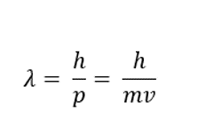
λ = wavelength
h = Planck’s constant
p = momentum
m = mass of particle
v = velocity of particle
When the electron beam is fired at a sample, some of the electrons in the beam will be repelled or ‘scattered’ by electrons within the atoms in the sample. However, most of the electrons from the beam will pass straight through the sample. It is these ‘transmitted’ electrons that can be used to create an image in transmission electron microscopy (TEM).
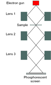
Electrons are produced by an electron gun at the top of the microscope column and accelerated down the column towards the sample by applying a voltage. It is crucial that the whole column is kept under a vacuum as the electron beam will be scattered easily by any air particles or contaminants within the microscope.
The beam is focused onto the sample using a set of lenses just like in a light microscope. However, rather than using glass lenses, each lens in a TEM is a coil of copper wire through which a current is passed. This generates an electromagnetic field that directs the beam in the right direction. Once the beam has passed through the sample, more lenses are used to focus and magnify the beam onto a phosphorescent screen that can be used to produce an image.
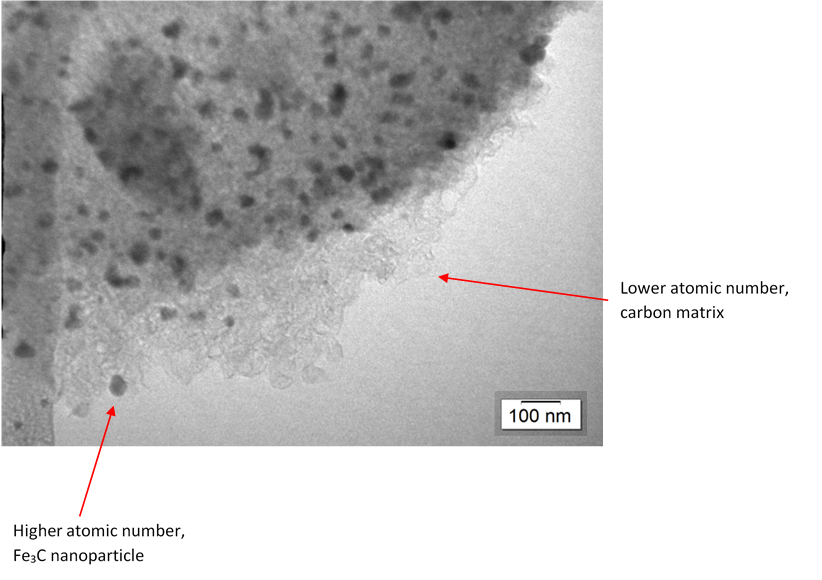
It is important to prepare a very thin sample, otherwise the electron beam will not be able to pass through it to produce an image. However, it is difficult to produce a truly 2D sample, so the user will be viewing a 2D ‘silhouette’ image of a 3D sample. This means that thicker areas of the sample will appear darker in the image.
Elements with higher atomic numbers will also appear darker because they contain more electrons, so they will scatter the electron beam more than elements with lower atomic numbers. TEM is therefore very useful for distinguishing regions of different electron density within the sample.
TEM has been found to be an extremely useful technique to scientists in various fields. Some of its applications include:
- Investigating defects in crystalline solids
- Researching nanomaterials
- Studying biological samples such as viruses and bacteria.
This work is licensed under a Creative Commons Attribution 4.0 International License.
